GPU Server Topology: NVLink, PCIe and NUMA
What NV#, PIX, PXB, PHB, NODE and SYS in nvidia-smi topo -m mean on the board of a two-socket GPU server, with two real machines.
- Doc no.
- KKZ-TN-151
- Date
- 2026-10-30
- GMT day
- 2026:303
- Est. read
- 10 min
$ nvidia-smi topo -m
        GPU0    GPU1    GPU2    GPU3    CPU Affinity    NUMA Affinity   GPU NUMA ID
GPU0     X      NV12    SYS     SYS     0,2,4,6,8,10    0               N/A
GPU1    NV12     X      SYS     SYS     0,2,4,6,8,10    0               N/A
GPU2    SYS     SYS      X      NV12    1,3,5,7,9,11    1               N/A
GPU3    SYS     SYS     NV12     X      1,3,5,7,9,11    1               N/A

Legend:
  X    = Self
  SYS  = Connection traversing PCIe as well as the SMP interconnect between NUMA nodes (e.g., QPI/UPI)
  NODE = Connection traversing PCIe as well as the interconnect between PCIe Host Bridges within a NUMA node
  PHB  = Connection traversing PCIe as well as a PCIe Host Bridge (typically the CPU)
  PXB  = Connection traversing multiple PCIe bridges (without traversing the PCIe Host Bridge)
  PIX  = Connection traversing at most a single PCIe bridge
  NV#  = Connection traversing a bonded set of # NVLinks
Each code says what a transfer between two GPUs passes through on the way. To read them, you need a picture of the board.
01The Output#
nvidia-smi topo -m output: the GPU-to-GPU matrix, then CPU affinity, NUMA affinity and GPU NUMA ID.- Connection type between two GPUs;
Xon the diagonal. - CPUs on the socket the GPU is attached to.
- The NUMA node of those CPUs.
- The NUMA node of the GPU’s own memory, only on systems like Grace Hopper;
N/Afor PCIe cards.
02The Board#
- NUMA node: one CPU and its memory.
- UPI: the link between the sockets (xGMI on AMD).
- HB (PCIe host bridge): where PCIe leaves the CPU. A modern CPU has several, joined by its on-die fabric.
- PCIe switch: fans one link out to several devices.
Inside a CPU, the cores and the memory controller talk over the on-die fabric (a mesh on Intel, Infinity Fabric on AMD), not PCIe. The host bridge, also called a root complex, sits between the two: it turns fabric traffic into PCIe and is the root of a PCIe tree. Its root ports are the links that leave the chip, each an x16 or x8 to a slot or a switch.
One host bridge drives only so many lanes, so a CPU has several: one per x16 group on Intel Xeon, one per quadrant on AMD EPYC. lspci -tv shows each as a separate root, such as [0000:40].
This board prints:
        GPU0    GPU1    GPU2    GPU3    NIC0
GPU0     X      PIX     NODE    SYS     SYS
GPU1    PIX      X      NODE    SYS     SYS
GPU2    NODE    NODE     X      SYS     SYS
GPU3    SYS     SYS     SYS      X      NODE
NIC0 SYS SYS SYS NODE X03The Codes#
From nearest to farthest. Orange is the path between the two highlighted GPUs.
3.1NV#: NVLink#
The GPUs talk over NVLink, not PCIe, and # is how many links the pair shares. On A100 one link carries 25 GB/s in each direction at the same time, so a pair gets # × 25 GB/s each way. NVIDIA’s spec sheets add the two directions: “600 GB/s” for A100 is 300 GB/s each way.
A GPU has a fixed number of links (12 on A100), so # depends on how the board spends them. Three ways:
| Code | Wiring | Per direction |
|---|---|---|
NV12 | 2 × A100 PCIe with 3 bridges | 300 GB/s |
NV12 | 8 × A100 on NVSwitch | 300 GB/s |
NV4 | 4 × A100, direct | 100 GB/s |
3.1.1Bridge pair#
NV12); GPU2 has no partner and uses PCIe only.A PCIe A100 card has 3 NVLink connectors on its top edge, 4 links each. A bridge is a small separate board that joins the same connector on two neighboring cards; a pair needs three of them, and they are sold as a set per pair. With all three, every link goes to the one partner: NV12.
A bridge only joins two cards, so a card has at most one NVLink partner. Every other GPU is reached over PCIe, and since NV12 takes the cell, the matrix no longer shows the PCIe path inside the pair. Machine 2 below is built this way.
3.1.2NVSwitch#
On an 8-GPU SXM board (HGX A100, as in DGX A100) no GPU is wired to another. There are 6 NVSwitch chips, and each GPU connects 2 links to each of them. A switch forwards traffic from any of its ports to any other, like a network switch.
When GPU0 sends to GPU5, it spreads the data over all 6 switches, and each forwards it to GPU5 over its own 2 links. All 12 links carry the transfer end to end, and the same holds for any other pair, so every cell is NV12.
All 8 GPUs can send at full speed at once, which is what all-reduce does. That is 8 × 300 GB/s, but spread over 96 links and 6 chips: each switch has 16 GPU ports and moves 400 GB/s in and 400 GB/s out, which it is built to do at full rate on every port.
3.1.3Direct#
Without switches, links are wired to fixed peers. A 4-GPU SXM board (HGX A100 4-GPU, as in DGX Station A100) wires every pair directly: 12 links over 3 peers is NV4. GPU0 can use only 4 links to reach GPU1; the other 8 lead elsewhere and sit idle.
Four GPUs is about the limit for this: with 8, each GPU would have 7 peers and fewer than 2 links per peer, which is why 8-GPU boards use switches. Like a bridge, NVLink hides the PCIe path: on this board GPU0 and GPU2 are on different sockets, which over PCIe would be SYS.
3.2PIX: one PCIe switch#
3.2.1PCIe switches#
A PCIe switch is a chip with one upstream port, wired to a CPU root port, and several downstream ports for devices (Broadcom PEX and Microchip Switchtec are the common ones). Like a network switch, it forwards each transfer to the right port, so devices below it can talk to each other without going through the CPU.
For GPUs it does three things:
- More GPUs per CPU. A CPU has a limited number of PCIe lanes. A switch fans one x16 out to 4–5 x16 slots, which is how 8- and 10-GPU PCIe servers are built. The cost: the GPUs below share one x16 to the CPU, so copies from host memory at the same time split about 32 GB/s (PCIe 4.0) between them.
- GPU to GPU without the CPU. Peer-to-peer between two GPUs on the switch stays inside it, at full x16, whatever the uplink is doing.
- GPU next to NIC. A NIC on the same switch can read GPU memory directly, again without the CPU (below).
Servers with 2–4 GPUs, like the two machines below, usually wire each GPU straight to a CPU root port, with no switch.
3.2.2Two GPUs on one switch#
PIX: two GPUs on one PCIe switch.Traffic turns around inside the switch: PIX.
3.2.3Multi-node training#
Two nodes with 8 GPUs each, after NVIDIA’s DGX A100 topology diagram:
- 8 GPUs on NVSwitch,
NV12between every pair. - 8 RDMA NICs, one per GPU, 200 Gb/s each: 25 GB/s, about one PCIe 4.0 x16.
- 2 CPUs, each with 2 PCIe switch groups. In a group, the 2 NICs (and an NVMe drive, not drawn) sit on the upper switch, and the 2 GPUs on a second switch below it.
- The NICs of all nodes join one InfiniBand network.
Every GPU uses two interfaces at once:
12 NVLinks to the NVSwitches
- NVLink only connects GPUs to GPUs
A PCIe x16 link to its PCIe switch
- NICs, CPUs and drives only speak PCIe
Here is nvidia-smi topo -m from a real 8 × A100 SXM4 server (2 × EPYC 7543), posted on NVIDIA’s developer forum: every GPU row, and below them the first two NIC rows. The other NIC rows follow the same pattern.
nvidia-smi topo -m on a real 8 × A100 SXM4 server (2 × EPYC 7543): every GPU row, plus the NIC0 and NIC1 rows.- The GPU block is all
NV12. - Each GPU has two
PXBNICs, its pair. NIC0–NIC7 are the 8 compute NICs. - NIC8 and NIC9, the two ports of the storage NIC, are
SYSto every GPU: that card hangs directly off a CPU. - GPU0 and NIC2 are on the same CPU but still
SYS. The server runs NPS=4, which splits each EPYC socket into 4 NUMA nodes (the NUMA column), andSYSmeans crossing a NUMA node boundary.
Why PXB and not PIX? In the NIC rows, NIC0 and NIC1 are PIX to each other, so the two NICs share one switch, while the GPUs sit one switch further down. The matrix shows it is two levels deep:
PXB: two switches apart, while NIC0 ↔ NIC1 share one switch (PIX).3.2.4Traffic by destination#
Which path GPU0’s data takes depends on where it goes:
| Destination | Path | Per direction |
|---|---|---|
| GPU in the same node | NVLink through NVSwitch | 300 GB/s |
| GPU in another node | PCIe switch → NIC → network → NIC → PCIe switch | 25 GB/s per NIC |
| Host memory | PCIe switch → CPU | about 32 GB/s |
The cross-node path in full, with GPUDirect RDMA, which lets a NIC read and write GPU memory directly:
- Node A’s NIC reads the data from GPU0’s memory, a PCIe peer-to-peer read. GPU and NIC share a switch, so it turns around inside the switch.
- The NICs send it across the network.
- Node B’s NIC writes it straight into GPU0’s memory, again inside the switch.
Neither CPU nor host memory is on the path. Without GPUDirect RDMA, both ends would stage the data in host memory, crossing the uplink to the CPU twice per node.
An all-reduce over the 16 GPUs uses both kinds of links: NVLink inside each node, and all 8 NICs in parallel between the nodes, each GPU through the NIC next to it. nvidia-smi topo -m lists the NICs as extra rows (NIC0, NIC1, …), and NCCL reads the same distances: when a NIC is too far from its GPU, NCCL skips GPUDirect RDMA and stages through host memory.
3.3PXB: several PCIe switches#
PXB: a path through several PCIe switches, still below the CPU.A tree of switches, still below the CPU.
3.4PHB: one host bridge#
PHB: up to the CPU and back down through two root ports of the same host bridge.Up to the CPU and back down, through two root ports of the same host bridge.
3.5NODE: two host bridges, one CPU#
NODE: across two host bridges of one CPU, over its on-die fabric.Also crosses the CPU’s on-die fabric. The usual case for two GPUs on one socket of a current server.
3.6SYS: across sockets#
SYS: across sockets, over UPI.Crosses UPI. Slowest path; GPU peer-to-peer often doesn’t work here, and copies go through host memory.
3.7Summary#
04Practical Examples#
4.1Machine 1: One GPU per Socket#
$ nvidia-smi topo -m
        GPU0    GPU1    CPU Affinity    NUMA Affinity    GPU NUMA ID
GPU0     X      SYS     0,2,4,6,8,10    0                N/A
GPU1 SYS X 1,3,5,7,9,11 1 N/ASYS).The two GPUs only meet over UPI. Note how the CPUs are numbered:
Even CPUs are on socket 0, odd ones on socket 1, so bind by NUMA node, not by CPU range:
CUDA_VISIBLE_DEVICES=0 numactl -N 0 -m 0 python run.py &
CUDA_VISIBLE_DEVICES=1 numactl -N 1 -m 1 python run.py &
Two independent jobs fit this machine well. Tensor parallelism across the two GPUs doesn’t: it all-reduces in every layer, over UPI.
4.2Machine 2: Two NVLink Pairs#
The output at the top of the post.
NV12 pairs, one per CPU; between the pairs is PCIe + UPI.A Dell R750xa: GPU0–1 on CPU0, GPU2–3 on CPU1. Each pair has three NVLink bridges (NV12, 300 GB/s per direction); between the pairs is PCIe + UPI.
- Tensor parallelism belongs inside a pair: TP=2 on {0, 1} and on {2, 3}.
- For a model that needs all four GPUs, TP=2 × PP=2 beats TP=4. With TP=4, every all-reduce crosses
SYSbetween the pairs and runs at PCIe + UPI speed.
4.3Machine 3: Eight GPUs, Two NUMA Nodes#
Another 8-GPU server. Here are its GPU rows and the NIC0 and NIC1 rows:
NV8, and only two NUMA nodes, so paths inside a socket read NODE.Drawn as hardware:
The groups are built as on the 8 × A100 server in Multi-node training: two GPUs and two NICs each, PXB from a GPU to its NICs and PIX between the two NICs. Three things differ.
First, the pairs are NV8, not NV12: 8 NVLinks, 200 GB/s per direction. That is the link count of A800 and H800, the export versions of A100 and H100; nvidia-smi -L tells which.
Second, there is one NUMA node per socket. GPU1 to NIC4, a NIC in the other group on the same CPU, reads NODE here. On the A100 server the same kind of path, from one host bridge over the fabric to another, reads SYS, because NPS=4 gives each host bridge a NUMA node of its own. Here only paths between the sockets are SYS.
Third, the extra NIC pair is NIC0 and NIC1, on CPU0, so the NICs of GPU0 are NIC2 and NIC3. NIC k is not necessarily GPU k’s: NCCL reads the matrix itself, but check it before setting NCCL_IB_HCA by hand.
- InfiniBand
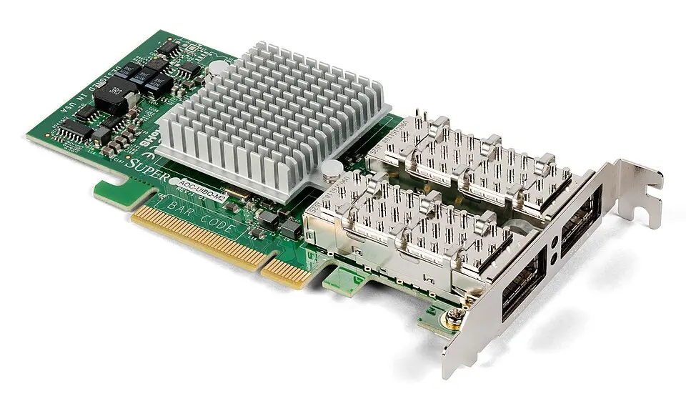
- A network standard, not a brand, built for clusters: it does not drop packets, and RDMA is built in, so a NIC can read and write another machine’s memory without its CPU. Nearly all InfiniBand gear comes from Mellanox, now part of NVIDIA. The NICs in DGX A100 run HDR InfiniBand at 200 Gb/s (25 GB/s) per port. Pictured: an older InfiniBand NIC, a PCIe card with two ports.↩Photo: Dmitry Nosachev, CC BY-SA 4.0, via Wikimedia Commons